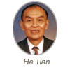
AWARDEE OF TECHNOLOGICAL SCIENCES PRIZE
TU HAILING
Dr.Tu Hailing, born in Beijing in October 1946, is a leading scientist of information functional materials. He graduated from Department of Radio and Automation, University of Tianjin in 1969, and attended School of Physics, University of Bath in UK in 1979 where he received a PhD in solid state physics in 1983. From 1994 to 1995, he was the visiting professor in Department of Materials Science and Engineering, North Carolina State University in US. He has been the chairman of the Managing Committee of National Engineering Research Center for Semiconductor Materials since 1991 and the president of General Research Institute for Nonferrous Metals since 1996.
He has been in charge of the semiconductor materials research projects of the 8th, 9th National Fiveyear Plan and the 10th 863 Hightech Program and held responsibilities for the national projects of the large diameter silicon polished wafers. Activities included developing a series of technologies for 6″ and 8″ silicon polished wafers, designing the new As doping facilities and modifying the hot zone configuration. He led his group successfully to grow 12″ silicon single crystal ingots with 24″ and 28″ hot zones, which was voted as one of the ten achievements of science and technology in China in 1997. His early research work involved the defects behavior in P(100) Si wafers, elimination of the stacking faults in N(100) Si wafers, evolution of oxygen precipitation in silicon, and effects of Fe contents on the minority carrier lifetime in Ptype silicon. He investigated multilayer structural siliconbased materials such as the silicononinsulator and strained silicon, and has found that germanium implantation followed by thermal annealing can reduce the density of crystal originated pits (COPs) in silicon wafers.
He has also made significant contribution to research and development of compound semiconductor materials. His group has designed the horizontal Bridgman (HB), the vertical magnetic field (VMCZ) and the vapor controlled Czochralski (VCZ) crystal growth furnaces and held China and US patents. With these furnaces, they have grown, for the first time in China, the 4″ VMCZ and VCZ GaAs crystals respectively. Dr. Tu has found that the transverse phonon mode softens with increasing of the vacancy concentration in ternary compound semiconductor materials and the critical phenomenon in the vicinity of phase transition induced by temperature, pressure and compositions in rare earth compound semiconductors is related to the electronphonon interaction. He and his group investigated the structural properties of semiinsulating GaAs wafers by trebleaxis Xray diffraction and synchrotron radiation Xray fluorescence, and it has been concluded that as vapor pressure and annealing processes can affect the defects, as precipitations and stoichiometry in GaAs.
He has been actively promoting the semiconductor hightech industry and responsible for accomplishing the silicon wafer production line with the capacity of 60 million square inches per year and the compound semiconductor materials production line with the capacity of 4 tons per year. Those products are currently sold on the domestic and international markets.
Dr. Tu has been lecturing at Tsinghua University, Beijing University of Science and Technology and several other universities. He has authored and coauthored more than 140 papers in the open scientific literature, which have been cited by SCI for more than 340 times. He has published 7 books, been granted 12 patents and won 14 national and provincial technological progress awards. His work was recognized with the distinguished contribution award from Semiconductor Equipment and Materials International in 2002.


