AWARDEE OF TECHNOLOGICAL SCIENCES PRIZE
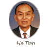
WANG ZHANGUO
Abstract
Wang Zhanguo was born on December 29, 1938.in Zhenping County, Henan Province, China. He joined the Institute of Semiconductors, Chinese Academy of Sciences (IS CAS) after graduating from department of physics, Nankai University, China. He is currently a professor of ISCAS, Director of Key Laboratory of Semiconductor Materials Science, ISCAS, and the standing director of Chinese Materials Research Society. From 1990 to May 2001 he was the member of National Advanced Materials Committee of China. He has been engaged in studies on semiconductor materials physics since 1962. From 1980 to 1983, he was as a visiting scientist at Department of Solid State Physics, the University of Lund, Sweden where he contributed to deep energy level physics and photoluminescence studies of semiconductors. He and his co-workers developed a new method to identify whether the two deep levels within a band gap are coupled or not, thus solving the long existing fundamental question of gold-related donor and acceptor in Si, and A and B deep levels in LPE GaAs. He suggested a model of deep level broadening and PL spectrum splitting in semiconductor alloys. According to this model, the non-exponential transient behavior of thermal emission and capture of carriers via deep levels and the physical origin of PL spectrum splitting of deep levels could be explained.
In 1986, he joined Professor Lin Lanying's group, and the GaAs single crystal was successfully grown from the melt in space for the first time. In 1993, he proposed a multi-level compensation model and new criteria of electrical compensation for undoped SI-GaAs, which can not only explain the GaAs conductivity but also provide a clue for improving the quality of this material.
From 1993 up to now, he and his co-workers are working on growth of semiconductor nanostructures, such as quantum well, quantum wires and quantum dots etc and the fabrication of quantum devices as well. Using molecular beam epitaxy technique and SK growth mode, through the stress distribution design of the materials system, controlling the growth dynamics and optimizing growth conditions, the uniformity and the density as well as the spatial ordering of In (Ga) As/GaAs, InAlAs/AlGaAs/GaAs and InAs/InAl (Ga) As/InP nanostructrues can be experimentally controlled, and free defects of quantum dots (QDs) and quantum wires have been obtained. High power QD lasers with continuous-wave output of 3.6W and the wavelength around 960nm operating at room temperature are also successfully fabricated from vertical coupled InAs/GaAs QDs ensemble, which is one of the best results published in literatures. Recently a concept of the flexible substrate was proposed by him, in which might open a new direction for developing new hetero-structural materials system with a large lattice mismatch.
He has published some 160 papers in many authoritative journals, and he was awarded a number of National and Chinese Academy of sciences Prizes.
He was elected the academician of the Chinese Academy of Sciences in 1995.


